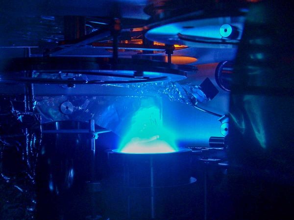
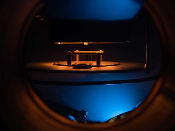
Magnetron sputtering is a versatile deposition technique used to create thin films on a substrate surface by sputtering atoms or molecules from a target material. It offers a good deposition rate and the ability to deposit a wide range of materials including metals, dielectrics, and semiconductors. In this process, an Argon plasma is ignited above a negatively biased and magnetized target material, drawing ions from the plasma towards the target material. As a result, Argon ions impact the target, causing atoms or molecules to be ejected from the surface through a process known as sputtering. The sputtered material forms a vapour that condenses on the substrate surface, resulting in the formation of a thin film
Applications
Magnetron sputtering can be used to deposit to create optical antireflective coatings, anticorrosive coatings, IR optics, dental protheses, and super-insulation. This deposition method is also employed in microelectronics for producing metal film capacitors, optical data storage, and microprocessors, as well as in the consumer industry for manufacturing anti-reflective coatings
Consumer Electronics
Automotive Industry
Solar Energy
Aerospace and defence
Healthcare and medical devices
Optics and photonics
Surface engineering
Key features
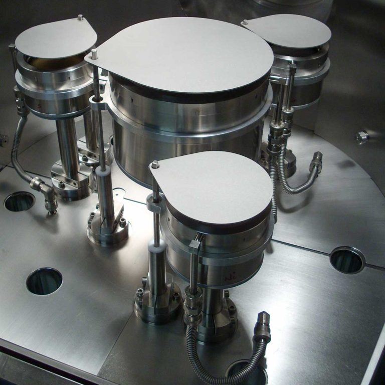
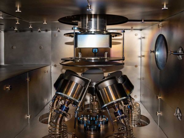
Single, vertical coplanar, confocal or linear configuration sources can be combined for DC, DC pulsed, RF, HIPIMS
Co-sputtering configuration
Reactive gases (02 , N2 , etc) can be added for direct reaction during deposition process
Integrated quartz crystal controller for thickness monitoring
Optional wide range optical thickness monitor for the control of layer thickness for a large number of layers by T% or R% monitoring on the coated substrates
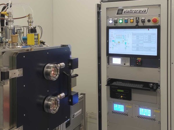
Software interface for real time deposition monitoring
Deposited materials
Metals, Oxides, Nitrides, Carbides, Semiconductors, Carbon Based Materials