Sputtering process


Ion Beam Sputtering
IBS
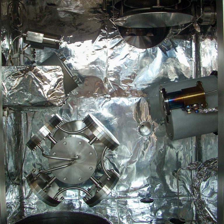
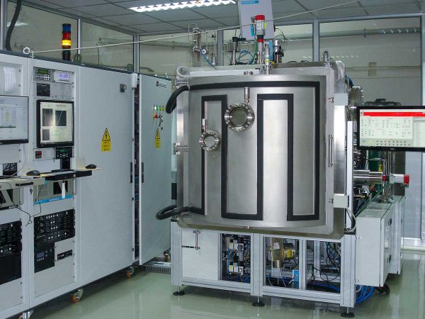
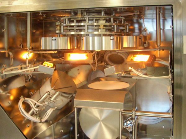
Ion Beam Sputtering (IBS) is a deposition technique that uses an ion source to sputter a target material onto a substrate. The system includes a rotary multitarget assembly, a substrate, and an ion source used to sputter the target and deposit it onto the substrate surface. Using gas (Ar) injection into the ion gun, a high electric field causes gas ionization, creating a plasma inside the source region. The ions generated in the plasma are accelerated from the source to the target, creating a collimated ion beam with a well-defined ionic energy and density. This beam impacts the target material, causing it to sputter towards the substrate. Plasma in IBS is confined within the ion source, allowing the chamber pressure to be maintained low. An additional ion beam source can be used to bombard the substrate with Ar ions to improve the density or reactive gas ions to maintain stoichiometry. Substrate heating during deposition can improve overall sputtering performance.

Applications
Ion beam applications encompass a wide range of processes that range over deposition, etching, or their combination. These applications include laser facet coating, mirrors for ring laser gyroscopes, X-ray optics, infrared sensors, telecom optic filters, Magnetic Random Access Memory (MRAM), dielectrics, spintronics, and superconductors
- Consumer Electronics
- Automotive Industry
- Aerospace and defence
- Healthcare and medical devices
- Optics and photonics
- Energy storage
Key features
- Low pressure processing (10-5 to 10-4 Torr range)
- Reduced porosity (higher density) in deposited films (low pressure means reduced included gas)
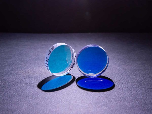
- High quality optical films with smooth surfaces
- Single Ion Beam or Dual Ion Beam configuration sources can be combined for DC, DC pulsed, RF depending on target material and layers that will be deposited
- Substrate conditioning from –35 °C up to 800 °C
- Reactive gases (02 , N2 , H2 , etc.) can be added for direct reaction during deposition process
- Optional automatic or manual load lock with optional pre-heating and/or plasma treatments
- Optional full optical thickness monitor for an unlimited number of layers by T% or R% wavelength scans on the coated substrates
Deposited materials
Metals, Oxides, Nitrides, Carbides, Semiconductors, Carbon Based Materials
Similar technologies

Ion Beam Sputtering
a robust solution enabling the widest range of deposited materials


