CVD Process


Atomic Layer Deposition
ALD
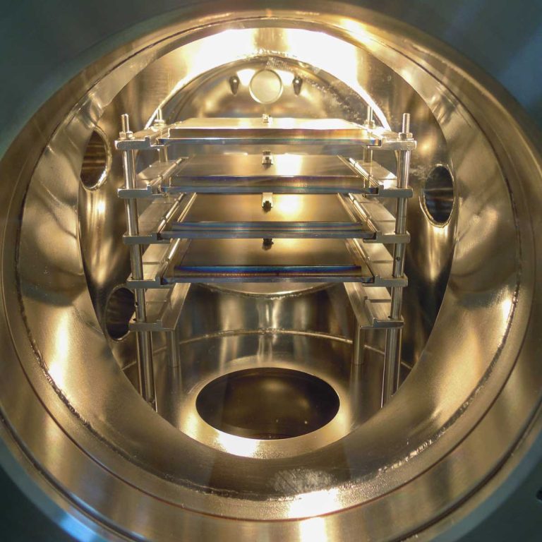
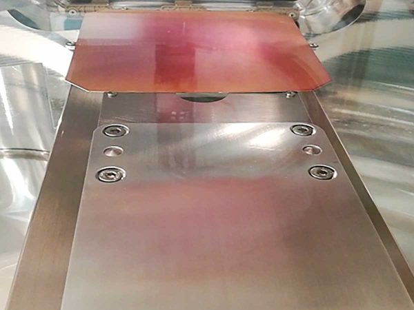
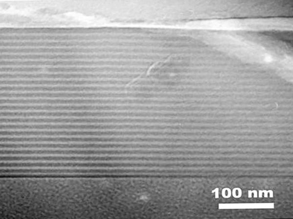
Atomic Layer Deposition (ALD) is a method of depositing thin films on a substrate surface through a chemical reaction between one or more reactive gases and the substrate. It is an advanced deposition technique that enables the deposition of ultra-thin films with exceptional precision. During ALD process, one or more reactive gases are introduced into a vacuum chamber, where they react with the substrate surface to deposit a thin film via a chemical reaction. This deposition method involves introducing gas phase precursors into the process chamber one by one, in a series of sequential, non-overlapping pulses. By reacting sequentially with the surface of the substrate, each precursor forms a self-limiting layer, and the reaction stops when all the reactive sites are consumed. Through repeated exposure to separate precursors, a thin film is slowly deposited

Applications
MOCVD is commonly used in the production of laser diodes, LEDs, and semiconductors for
advanced optoelectronics, high power and highspeed electronics, enabling mass production of semiconductor heterostructures via bandgap engineering. Furthermore, MOCVD can be utilized to precisely fabricate 0D, 1D, and 2D nanomaterials.
- Consumer Electronics
- Solar energy
- Aerospace and Defence
- Healthcare and medical devices
- Optics and Photonics
- Power Electronics
- Research
Key features
- Vapor source controllers for liquid Precursors with tank/cylinder in a closed cabinet for safe refill
- High speed pulsed valves for alternating precursor delivery
- Single or multiple furnaces in Hot Wall or Quartz Tube configuration
- Reactive gases (SiH4 , NH3 , H2 , CH4 , N2 , etc.) and/ or liquid precursors controlled directly from the software
- Optional load lock with pre-heating and/or plasma treatments
- Optional Plasma Enhanced configuration
- Optional Emission Spectrometer for in-situ plasma diagnostics and End Point Detection
Deposited materials
Oxides, Nitrides, Carbides, Semiconductors, Carbon Based Materials, Organics
Similar technologies

Atomic Layer Deposition
the most advanced choice for obtaining compound materials mixing gaseous and liquid precursors


